Two Ways to Go Vertical: Stanford’s Monolithic 3D Chip and Huawei’s LogicFolding
Two of the most-watched scaling announcements of the last year both went up instead of smaller. That’s the part worth sitting with. Flat 2D scaling has been getting expensive and slow for a while, and the two camps that grabbed headlines in late 2025 and mid-2026 both answered the same way — stack the silicon, shorten the wires — while sitting at opposite ends of the evidence spectrum.
One is a fabricated, measured, peer-reviewed chip out of a Stanford-led team, built in a commercial US foundry and presented at IEDM. The other is an announced design methodology plus a rebranded scaling metric out of Huawei, with first silicon pending and no independent measurement. Both are going vertical. Only one of them you can currently check.
That asymmetry is the whole point of putting them side by side, so I’m going to keep it loud throughout. Stanford’s numbers are measured; I’ll say measured. Huawei’s numbers are Huawei’s claims; I’ll say claims. If that reads as me being harder on Huawei, it’s not editorializing about geopolitics — it’s that one party fabricated a part and let people probe it, and the other showed slides.
What Stanford actually built
The Stanford line of work — this is the N3XT research program, with Subhasish Mitra as PI and Tathagata Srimani (now CMU) as senior author, plus collaborators at UPenn, MIT, and SkyWater — produced what’s described as the first monolithic 3D (M3D) chip fabricated in a commercial US foundry. It went to IEDM 2025 in December, session 28-5. Not a press release. A device meeting where people ask hard questions.
The engineering detail the consumer coverage mostly skipped is the interesting bit. This is heterogeneous integration: silicon CMOS, resistive RAM (RRAM), and carbon nanotube field-effect transistors (CNFETs), with the upper tiers built in the back-end-of-line at 415 °C or below. That temperature ceiling is the enabler for the entire approach. Build your upper tiers too hot and you cook the circuitry already sitting underneath them. Keep the thermal budget low enough and you can fabricate tier on tier, sequentially, on one wafer, and wire them together far more densely than you could ever bond.
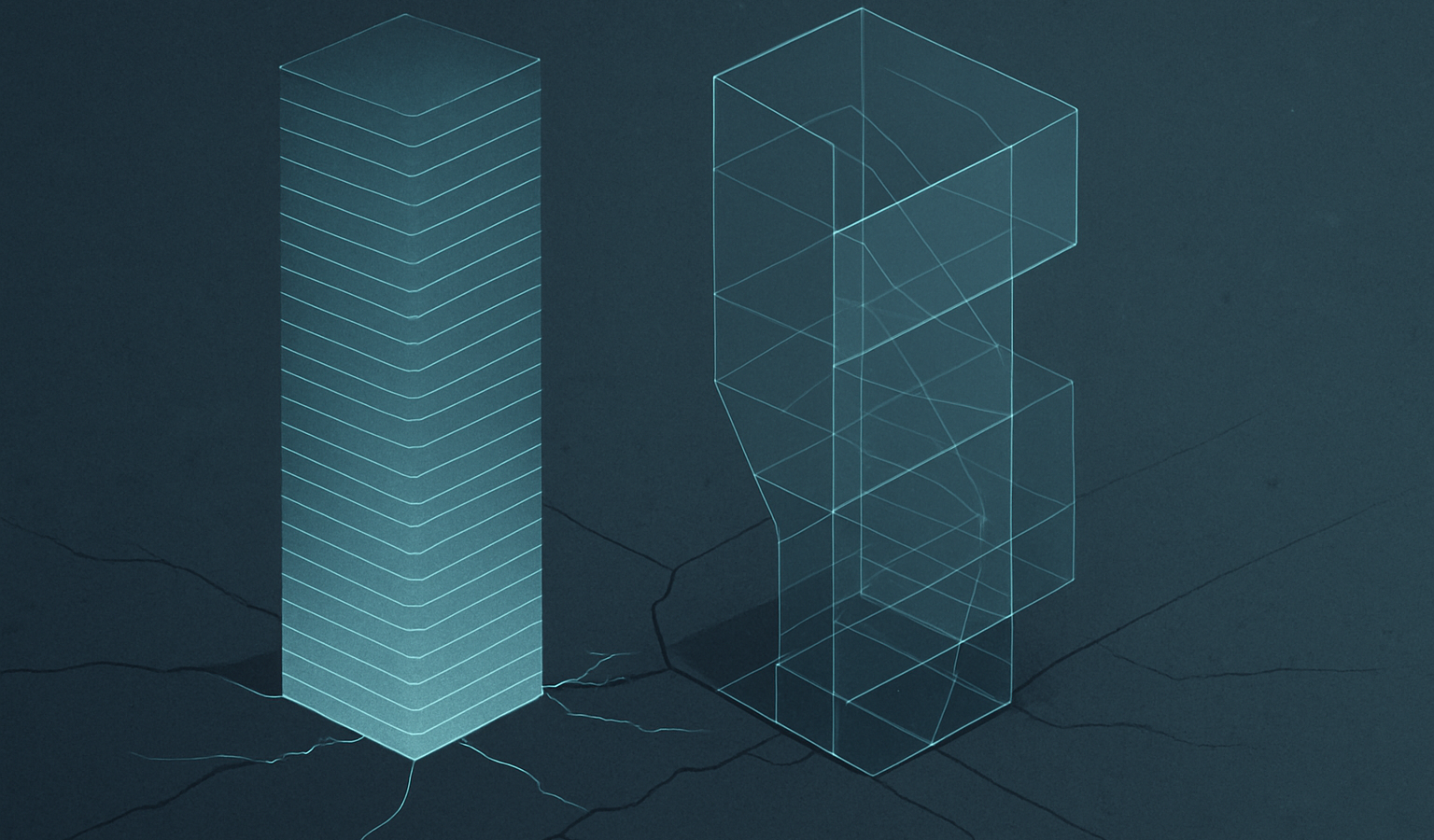
Which gets at the distinction that matters here. Monolithic 3D is not the same thing as the “3D” in most marketing decks. Conventional 3D bonds separate dies and connects them with through-silicon vias — relatively few vertical links, relatively coarse. Monolithic 3D grows the tiers in place, so you get orders of magnitude more, finer-grained vertical connections between layers. The density of that vertical wiring is the product. A specific design feature the team highlighted: full M3D memory arrays with sense amplifiers tucked in to drive the logic directly above and below them.
The manufacturing story is almost the headline by itself. SkyWater Technology in Bloomington, Minnesota — pitched as the largest exclusively US-based pure-play foundry — ran this on a mature 90/130 nm node, 200 mm wafers. Old node. Real commercial flow. The argument being made isn’t “we found a magic process,” it’s “this architecture transfers into domestic manufacturing on tooling that already exists.” For anyone tired of every scaling story requiring the next EUV scanner, that framing lands.
Now the results, and I’m keeping measured and simulated in separate boxes because the team did too.
| Figure | Status | Notes |
|---|---|---|
| ~4× vs comparable 2D | Measured (hardware prototype) | Compute throughput / read bandwidth |
| ~12× | Simulated | More-tier designs on AI workloads derived from Meta’s open LLaMA models |
| 100–1000× energy-delay product | Aspirational target | Long-term, not a result |
Lead with the ~4×. That’s the hardware. The ~12× is a simulation of a deeper stack, the 100–1000× EDP number is a target on a slide, and conflating the three is exactly how a clean measured result turns into hype by the third reblog.
What it’s for is the memory wall. On a flat chip, compute keeps outrunning the chip’s ability to feed it data, and that data has to travel a handful of long, congested routes to get from memory to logic. Stack the memory directly over the logic and you do two things at once: shorten the trip and add a lot of parallel vertical lanes. Throughput up, energy per operation down, same move. The named target application is AI and LLM inference — the writeups reach for ChatGPT and Claude as the workload shape.
Give it its due, then name the caveats. It’s measured, it’s foundry-real, it’s transparent. But it’s a research-scale prototype on a 90/130 nm node, and CNFET plus RRAM at volume yield is its own unsolved problem — getting carbon nanotube transistors to behave consistently across a 300 mm production wafer is not a thing anyone has demonstrated at scale. The architecture is real. The road to a product on it is long.
What Huawei announced
Different register entirely. At IEEE ISCAS 2026 in Shanghai on May 25, He Tingbo presented two things: a scaling framing Huawei calls the Tau (τ) scaling law, and a design technique called LogicFolding.
The Tau pitch is that the industry should stop optimizing for feature size and start optimizing for time — how fast signals propagate across the system — and treat that as the successor metric to Moore’s Law. As a framing it’s not crazy. Wire delay has dominated transistor delay for a long time, and “smaller transistor” has been a weak proxy for “faster system” for a while. As a law it’s marketing, but the underlying observation about interconnect being the bottleneck is sound.
LogicFolding is the concrete part, and here you have to be careful about who said what. Huawei’s own release is thin on mechanism. The cell-level, dual-layer description — folding a circuit’s standard cells across stacked layers at the design stage, cell-to-cell rather than die-to-die packaging, to shorten critical-path wiring and raise effective density — comes from Tom’s Hardware’s reporting, not from Huawei primary. So attribute the mechanism to the reporting. Conceptually it’s a logic-on-logic vertical fold, which is a genuinely different target from Stanford’s memory-on-logic stack.
The numbers, all Huawei’s, all presented without a replication methodology anyone outside Huawei can run:
- A 53.5% transistor-density increase, given as 155 → 238 MTr/mm². Some outlets round to 54% or 55%; the precise figure stated was 53.5%.
- 41% better energy efficiency on performance cores.
- Peak clock of 3.1 GHz.
- All of it claimed without EUV — without the advanced lithography export controls deny China.
The roadmap is a separate thing from the numbers, and it’s where the skepticism should anchor. Huawei says chips designed under the τ law are expected to reach density equivalent to 14 Å (1.4 nm) by 2031. That’s a projection, explicitly. Analysts note it lands roughly three years past TSMC’s stated 1.4 nm timeline. Huawei also says it has “designed and mass-produced 381 chips” over six years under this approach — a claim offered without metrics, so do with it what you will.
First silicon is the near-term thing to actually watch. He Tingbo said the next Kirin SoC — reported as the Kirin 9050 Pro in the Mate 90 series, around September 2026 — will be the first commercial part to adopt LogicFolding. And here’s the distinction the breathless coverage blurred: that autumn chip is reported as a 3nm-class part. It is not the 1.4 nm claim. The 1.4 nm-equivalent is the 2031 projection. As of the announcement nothing using LogicFolding had shipped, so every density and efficiency figure above is a pre-product claim.
The manufacturing logic is the whole reason this exists. Export controls cut Huawei off from EUV. So the entire pitch is to get density gains from design — vertical folding, shorter interconnect — and stay on DUV-based processes it can actually access, meaning SMIC’s roughly 7nm-class line, rather than the EUV it can’t buy. As an idea, that’s legitimate. Density from architecture instead of lithography is exactly the kind of move a tooling-constrained player should make.
The open question, flagged by analysts and worth surfacing rather than burying, is manufacturability — yield and cost. Folding logic across layers without advanced tooling is hard, and Huawei has not shown it can produce 1.4nm-equivalent parts at scale. TechTimes and others put it plainly: a 53–54% density gain claimed, no independent audit yet. semiconalpha’s skeptical writeup frames the read as desperation, a genuine breakthrough, or both — and honestly that’s the right posture. Unproven until the Mate 90 silicon gets independently measured. If the autumn part ships and someone delayers it and the density holds up, the story changes. Until then it’s a slide deck with a phone attached to it.
How they differ
Start with what’s being stacked, because that’s the cleanest line between them. Stanford integrates heterogeneous memory and logic tiers — Si CMOS, RRAM, CNFET — to kill the memory wall. Huawei folds logic onto logic to raise density and shorten wiring. Memory-centric versus logic-centric. They’re solving adjacent problems, not the same one.
The goals diverge from there. Stanford is chasing throughput and energy-per-operation for AI inference — a data-movement problem. Huawei is chasing density parity without EUV — a tooling-and-sanctions problem — wrapped in a re-framed scaling metric. One is a physics-and-architecture play; the other is a physics-and-architecture play with a geopolitical forcing function bolted to the front of it.
And then the evidence, which is the gap that should govern how you read both. Stanford: fabricated, measured at ~4×, peer-reviewed at IEDM, built in a commercial US foundry on a mature node, openly benchmarked with measured and simulated numbers kept distinct. Huawei: announced, projected, first silicon pending in autumn 2026, no independent audit, mechanism details sourced to reporting rather than the primary release. A measured result versus a claim plus a roadmap. Don’t let anyone flatten that into “two competing 3D approaches” as if they sit on equal footing. They don’t, not yet.
Maturity and motivation cut the other way, to be fair about it. Stanford is academic, transparent, and benchmarked — but it’s research scale on a 90/130 nm node, years from a product. Huawei is commercial, near-term, shipping a phone this autumn, and motivated by a real constraint — but unverified. The thing you can check is far from market; the thing near market you can’t check.
What they share is the part that actually matters for where compute is going. Both reject “smaller features is the only path.” Both go vertical. Both attack the interconnect and data-movement bottleneck by shortening wires rather than shrinking transistors. And both implicitly argue that the next decade of scaling is the third dimension plus architecture, not lithography alone. That convergence — two of the most-watched 2026 moves both going up instead of smaller, from a US university foundry collaboration and a sanctioned Chinese vendor respectively — is the real signal. The wall is the same. The directions agree. The evidence bars don’t.
Watch two things. Whether anyone can take Stanford’s M3D off a mature node and toward a real process with CNFET/RRAM yield that survives volume. And whether the Mate 90 ships and the LogicFolding density claim holds up under independent measurement. Two clocks, both running, neither stopped.
Sources
- IEDM 2025 session 28-5 listing (IEEE IEDM)
- Scientists and a US foundry achieve a 3D chip breakthrough to accelerate AI (Stanford Engineering)
- Stanford-led team builds 3D AI chip at US foundry, reports 4x performance gains (Tom’s Hardware)
- New 3D chip stacks memory and logic (ScienceDaily)
- This new 3D chip could shatter the memory wall holding back AI (SciTechDaily)
- Huawei unveils Tau scaling at IEEE ISCAS (Huawei)
- Huawei claims sanctions-busting breakthrough with 1.4nm-class chips by 2031, introduces LogicFolding and Tau scaling (Tom’s Hardware)
- Huawei unveils new scaling law and tech to develop 14 nm-equivalent chips by 2031 (SCMP)
- Huawei’s Mate 90 series expected to debut new Kirin chip this autumn (TechNode)
- Huawei LogicFolding chip claims 54% density gain: no independent audit yet (TechTimes)
- Huawei’s Tau scaling law and LogicFolding (semiconalpha)